 仕事内容
Rapidus is a leading foundry at the forefront of semiconductor innovation, enabling the next generation of integrated circuits. We are seeking a highly skilled and experienced Test Chip Design Engineer to join our team. In this role, you will be responsible for the physical design and PPA (Power, Performance, Area) analysis of cutting-edge test chips, critical for validating and characterizing our advanced process technologies.
You will play a pivotal role in bridging the gap between process development and product design, ensuring our technology offerings meet the demanding requirements of our global customers. This position offers a unique opportunity to work with the latest process nodes and design methodologies, contributing directly to the future of semiconductor manufacturing.
Key Responsibilities
As a Test Chip Design Engineer, your responsibilities will include:
- Test Chip Physical Design and PPA Analysis:
- Backend (BE) Implementation and Related Flow Development: Drive the full backend implementation flow, from chip-level planning and PG (Power/Ground) network design to floorplan, place, CTS (Clock Tree Synthesis), route, power analysis (PDNA sign-off), and comprehensive physical verification.
- Design Methodology and EDA Tool Utility Development: Develop and enhance design methodologies and associated EDA tool utilities specifically for backend implementation. This includes creating solutions for challenges arising from new process technologies and developing utilities to support our customers effectively.
- Technology Benchmark: Conduct detailed technology benchmarking to thoroughly understand and evaluate the PPA characteristics of new process technologies.
- Collaborate closely with process development teams, circuit design teams, and EDA vendors to define and implement robust design flows.
- Analyze and debug complex physical design issues, including timing, power, and physical verification failures.
- Contribute to the continuous improvement of design processes and methodologies.
- Document design specifications, methodologies, and results clearly and concisely.
 経験・資格
●Required Skills&Experience :
- Bachelor's degree or higher in Electrical Engineering, Electronics Engineering, or a related field.
- hands-on experience in digital backend IC design, with a strong focus on physical design and sign-off.
- Proven expertise in the full physical design flow: floorplanning, power grid design, placement, clock tree synthesis (CTS), routing, and physical verification (DRC/LVS/Antenna).
- Solid experience with power analysis (PDNA sign-off) and static timing analysis (STA).
- Proficiency with industry-standard EDA tools for physical design (e.g., Cadence Innovus, Synopsys Fusion Compiler, PrimeTime, RedHawk, Calibre).
- Experience in scripting languages (e.g., Tcl, Python, Perl) for design automation and flow development.
- Strong understanding of advanced CMOS process technologies and their impact on physical design.
- Excellent analytical and problem-solving skills, with a keen eye for detail.
- Business-level English proficiency, capable of technical discussions with international engineers.
- English communication skills.
●Preferred Skills&Experience
- Experience in test chip design or IP development within a foundry environment.
- Familiarity with advanced technology nodes (e.g., 7nm, 5nm, 3nm).
- Knowledge of FinFET or GAAFET architectures.
- Experience with custom layout design or standard cell library development.
- Prior experience in developing custom design methodologies or CAD utilities.
- Understanding of reliability issues (e.g., EM, IR drop, ESD) from a physical design perspective.
- Project leadership or mentoring experience.
●Desired Personality Traits
- Proactive and self-motivated, with a strong drive to innovate and solve complex technical challenges.
- Highly collaborative, able to work effectively with cross-functional teams across different geographies.
- Detail-oriented and committed to delivering high-quality, reliable designs.
- Continuously eager to learn and adapt to new technologies and methodologies.
- Strong communication skills to articulate complex technical concepts clearly.
 勤務地
 想定年収
 福利厚生・待遇
 勤務条件
フレックスタイム制(フルフレックス)
・1日の標準労働時間 7時間30分
・標準労働時間帯 9:00~17:30/08:30~17:00(休憩60分)
※時差勤務あり
・完全週休2日制(土・日)、国民の祝日
・年次有給休暇(20日 入社初年度は入社した月に応じる日数の年次有給休暇を付与する)
・創立記念日(8/10)
・年末年始休暇
・慶弔休暇
・産前・産後休暇
・育児休暇
・介護休暇
※年間休日 128日
3か月(労働条件は本採用と同じです)
昇給:有
・健康保険
・厚生年金
・雇用保険
・労災保険
 Recruiting No.
 社名
 事業内容
 設立
 資本金
 従業員数
 決算月
 平均年齢


【総合重電機メーカー直系 老舗コンサルティング会社】 先端テクノロジー・データサイエンス分野のコンサルタント
【東証プライム上場 世界に展開する電子・機械部品メーカー】 東京本部 セールスユニット センシングデバイスの提案営業・開発営業

【東証プライム上場 世界に展開する電子・機械部品メーカー】 半導体製品の営業・海外営業支援












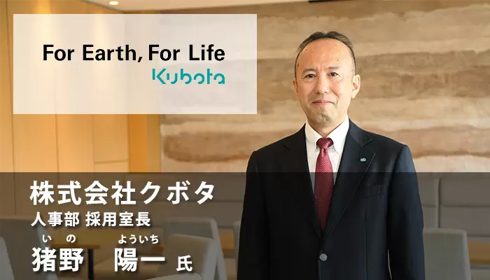
人々の生活や命を支えるため、「食料・水・環境」分野で地域に根ざした事業にチャレンジする
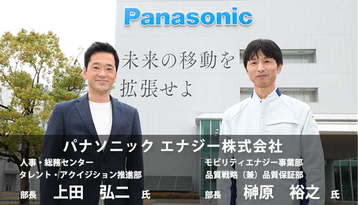
人の営みと地球環境が調和できる社会。 車載電池は一つの有効な手段になる。
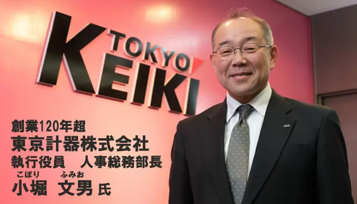
創業120年超、蓄積された技術資産を活用し、 多様な領域でトップクラスのシェアを確立。 グローバル事業の拡大も加速させています。
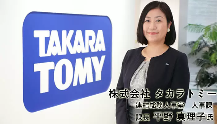
子どもたちに愛され続け、進化するおもちゃたちが、日本から世界へ、新しい夢と感動を広げています。

「夢に見るほど電池が好き」 な社員たちが、化学・電気・機械のノウハウを結集し、次世代エネルギーデバイスの開発に挑む。
世界の食料生産とエネルギー変換の分野で、ディーゼルエンジンの用途を広げています。


