 仕事内容
●Job Description
We are seeking a highly motivated and experienced Senior DFT Engineer to join our Enablement Team supporting the development of advanced semiconductor process technologies at the 2nm node and beyond. You will lead the Design-for-Test (DFT) implementation of large-scale test chips that are critical for enabling and validating our next-generation manufacturing processes.
In this role, you will focus on scan insertion, ATPG, memory BIST, and other DFT methodologies, while also supporting yield analysis and EDA tool collaboration to improve design quality and test efficiency. You will work closely with RTL designers, physical design teams, process integration engineers, and EDA partners to ensure robust DFT infrastructure across our global sites.
●Responsibilities
・Define and implement DFT architectures for technology development test chips, focusing on scan, boundary scan, and memory BIST.
・Function and timing verification of implemented DFT circuit, evaluate test coverage with DFT simulation (ATPG, BIST, Fault simuation).
・Propose the best test solution with analysis among test coverage, test cost, test time
・Collaborate with design teams to integrate DFT features from RTL through physical implementation.
・Develop and validate ATPG and MBIST patterns; support test bring-up and debug on silicon.
・Analyze test data from silicon to identify systematic issues and improve process yield.
・Engage with EDA vendors to evaluate and improve DFT tools and methodologies for advanced nodes.
・Document best practices and contribute to the enablement of scalable DFT flows across future technology nodes.
・Support cross-functional teams spanning design, process, product engineering, and reliability.
 経験・資格
●Minimum Qualifications
・MS or PhD in Electrical Engineering, Computer Engineering, or a related field.
・DFT development, preferably including advanced node designs or large-scale test chips.
・Strong expertise in scan-based DFT, ATPG, compression, and memory BIST techniques.
・Hands-on experience with commercial DFT tools (e.g., Synopsys TestMax, Siemens Tessent, Cadence Modus).
・Understanding of RTL-to-GDS flows and DFT timing considerations.
・Practical experience in silicon bring-up, failure analysis, and yield improvement.
・Excellent communication skills and the ability to work in a cross-site, cross-functional team.
●Preferred Qualifications
・Experience with DFT implementation for sub-5nm technologies.
・Experience with DFT implementation for chiplet SOCs.
・Familiarity with data analysis tools and methodologies used in yield learning.
・Strong scripting ability (Python, Tcl, Perl) for automation of DFT and test flows.
・Knowledge of test chip development for process technology enablement.
・Japanese language proficiency is a plus but not required.
 勤務地
 想定年収
 福利厚生・待遇
 勤務条件
フレックスタイム制(フルフレックス)
・1日の標準労働時間 7時間30分
・標準労働時間帯 9:00~17:30/08:30~17:00(休憩60分)
※時差勤務あり
・完全週休2日制(土・日)、国民の祝日
・年次有給休暇(20日 入社初年度は入社した月に応じる日数の年次有給休暇を付与する)
・創立記念日(8/10)
・年末年始休暇
・慶弔休暇
・産前・産後休暇
・育児休暇
・介護休暇
※年間休日 128日
3か月(労働条件は本採用と同じです)
昇給:有
・健康保険
・厚生年金
・雇用保険
・労災保険
 Recruiting No.
 社名
 事業内容
 設立
 資本金
 従業員数
 決算月
 平均年齢


【東証プライム上場 世界に展開する電子・機械部品メーカー】 東京本部 セールスユニット センシングデバイスの提案営業・開発営業

【東証プライム上場 世界に展開する電子・機械部品メーカー】 半導体製品の営業・海外営業支援
【東証プライム上場 財閥系 有名シンクタンク】 技術コンサルタント(先端技術調査・分析)







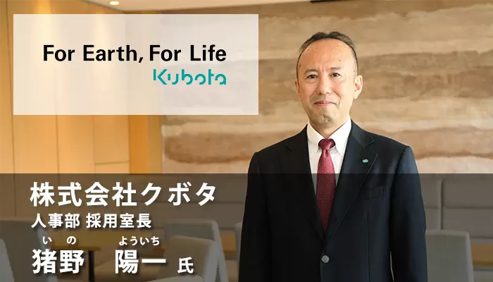
人々の生活や命を支えるため、「食料・水・環境」分野で地域に根ざした事業にチャレンジする
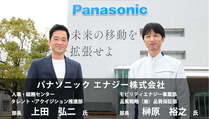
人の営みと地球環境が調和できる社会。 車載電池は一つの有効な手段になる。
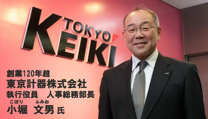
創業120年超、蓄積された技術資産を活用し、 多様な領域でトップクラスのシェアを確立。 グローバル事業の拡大も加速させています。
子どもたちに愛され続け、進化するおもちゃたちが、日本から世界へ、新しい夢と感動を広げています。

「夢に見るほど電池が好き」 な社員たちが、化学・電気・機械のノウハウを結集し、次世代エネルギーデバイスの開発に挑む。
世界の食料生産とエネルギー変換の分野で、ディーゼルエンジンの用途を広げています。


